<Points in this study>
- Transistors*2 on a gallium nitride (GaN) *1 layer bonded onto a diamond substrate were successfully fabricated after 800℃ thermal treatment, by utilizing a 3C-SiC bonding interface.
- Improvement in heat dissipation by the use of diamond compared to silicon was successfully demonstrated.
- Adopting high-quality 3C-SiC layers for the bonding.
- By using this technique, high-performance transistors on large-diameter gallium nitride-on-diamond substrates can be realized for the first time, which accelerates the social implementation of this technological field.
1. Overview
A research group composed of Dr. Keisuke Kawamura of Air Water Inc., Specially Appointed Associate Professor Jianbo Liang and Professor Naoteru Shigekawa of the Graduate School of Engineering, Osaka City University (since April 1, 2022, Osaka Metropolitan University) has succeeded in fabricating transistors using a gallium nitride layer that is bonded on a diamond substrate. This device process includes 800℃ thermal treatment. Improvement in heat dissipation by the use of diamond compared to silicon was also successfully demonstrated. This work was conducted in cooperation with Specially Appointed Associate Professor Yutaka Ohno and Professor Yasuyoshi Nagai from the Institute for Materials Research, Tohoku University, Dr. Yasuo Shimizu from the National Institute for Materials Science (at the time of this research) and other researchers.
GaN-based transistors are widely used in mobile base stations for cellular phones as next-generation semiconductors replacing silicon-based transistors. However, heat generation during operation greatly limits their performance, and large heat-dissipation components are required for their structure.
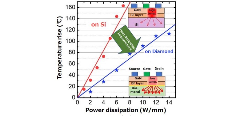
Fig. 1 Enhanced effect of heat dissipation performance realized by fabricating a transistor on a diamond substrate. (Better heat dissipation performance than that observed on a Si substrate produces a smaller temperature rise with the same power consumed.) (Data courtesy of Osaka Metropolitan University.)
This study has succeeded in forming surface-activated bonding between a diamond substrate and a gallium nitride layer by using a thin layer of silicon carbide (3C-SiC). The study has also succeeded in fabricating transistors with excellent heat dissipation performance by using the bonded substrate described above. Heat treatment at approx. 800℃ was performed during the manufacture of transistors; however, the bonding interface formed by 3C-SiC was so robust that the bonding interface did not suffer from exfoliation during the heat treatment. The transistors manufactured this time use diamond, the material that has the highest thermal conductivity on Earth and hence can dissipate heat the most effectively. It has been made clear that the use of diamond results in enhanced heat dissipation performance in comparison with transistors on silicon (Fig. 1) and that the quality of the gallium nitride layer does not degrade in this structure.
Since this study enabled fabrication of transistors after bonding processes, it is expected that commercialization of large diameter gallium nitride on diamond substrates will advance. Furthermore, it is also expected that this progress will enable gallium nitride-on-diamond technologies to pave the way for high-power applications such as radar and inverters*3. The results of this study were published online in Applied Physics Express, an international academic journal, on Tuesday, March 8, 2022.
2. Background
The degradation of performance and shortening of device service life due to heat generation and temperature rise during transistor operation pose a serious problem in their practical use. In particular, gallium nitride (GaN) transistors operate at higher outputs and at higher frequencies than do silicon (Si) transistors, which are mainstay transistors at present, so the development of effective techniques for heat dissipation is indispensable. As one of the solutions, various organizations have targeted and studied the realization of the ‘GaN-on-diamond’ structure, which uses diamond as a heat-spreader material. In particular, R&D using bonding technologies was actively pursued in this field of technology. These previous efforts, however, were unable to attain sufficient bonding strength, so that the ‘device-first process’, in which diamond substrates are bonded after transistor fabrication, has been the only way to realize gallium nitride (GaN) transistors on diamond substrates. This limitation of the process led to difficulty in enlarging the substrate diameter.
3. Details of this study
An 8-μm-thick gallium nitride layer and a 1-μm-thick silicon carbide (3C-SiC) buffer layer beneath the gallium nitride, grown on an Si substrate, were separated from the Si substrate and bonded onto a diamond substrate by using the surface-activated bonding method*4 (Figs. 2 (a) and (b)). After the bonding processes, gallium nitride transistors were manufactured of which processes include heat treatment at 800℃ (based on the bonding-first process) (Fig. 2 (c)). Using a high-quality silicon-carbide layer has allowed a satisfactory bonding interface free from exfoliation of the membrane, even after going through transistor-fabricating processes, to be realized as shown in the cross-sectional SEM*5 image (Fig. 2 (d)).
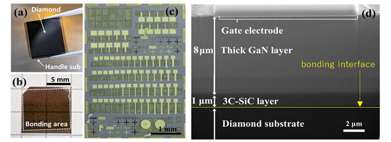
Figs. 2 (a) and (b): gallium nitride layer/diamond bonding sample. Figs. (c) and (d): transistor manufactured from a gallium nitride layer on a diamond substrate ((c): optical microscope image; (d): cross-sectional SEM image of the gate electrode section). (Data courtesy of Osaka Metropolitan University.)
To ascertain that the bonding onto a diamond substrate does not degrade the electric characteristics of a gallium nitride layer (the 2-dimensional electron mobility and the 2-dimensional electron concentration), characteristics comparisons were made with gallium nitride transistors manufactured in the same shape on Si substrates. The results have demonstrated that the rise in device temperature observed when the same amount of electricity was introduced was reduced to approx.1/3 on a diamond substrate compared to a Si substrate (improvement of heat dissipation characteristics) and that this reduction improved transistor characteristics.
4. Expected effects and future development
Fabricating transistors after the bonding process enables the diameter of gallium nitride layer bonded onto a diamond substrate to increase. As heat dissipation characteristics of gallium nitride transistors and integrated circuits improve, the scope of applications for the new transistors is expected to expand into high-output and high-power applications, such as radar units and inverters.
<Explanation of terms>
*1 Gallium nitride … Compared with silicon, gallium nitride enables a larger amount of power to be handled at higher frequencies. Since the 2014 Nobel Prize for Physics was awarded to three researchers who had been engaged in this field, gallium nitride-based semiconductors have been widely used in LED lighting and base stations for cellular phones.
*2 Transistor … A semiconductor element that controls the flow of electrons; it is capable of amplifying and switching signals.
*3 Inverter … A power electronics circuit that converts DC power into AC power. Inverters are widely used for electrically powered trains, air conditioners, and the like.
*4 Surface-activated bonding method … A method of bonding in which the surfaces of two samples are irradiated with beams of argon atoms in a vacuum (surface activation) and as is, the samples are brought into close contact with each other under the application of a load.
*5 SEM … A technique by which the structure of a sample under a scanning electron microscope is evaluated on the basis of the order of micrometers (1 μm = 10-6m).
Information on the journal carrying this paper
[The journal in which the paper was published] Applied Physics Express (IF = 2.895)
[The name of the paper] AlGaN/GaN/3C-SiC on diamond HEMTs with thick nitride layers prepared by bonding-first process
[Authors] Ryo Kagawa, Keisuke Kawamura, Yoshiki Sakaida, Sumito Ouchi, Hiroki Uratani, Yasuo Shimizu, Yutaka Ohno, Yasuyoshi Nagai, Jianbo Liang, and Naoteru Shigekawa
[URL for the paper] https://iopscience.iop.org/article/10.35848/1882-0786/ac5ba7
[Inquiries concerning the news release]
K. Kitahara, SIC Division, Air Water Inc.
2290-1, Takibe, Toyoshina, Azumino, Nagano, 399-8204, Japan
Telephone: +81-263-71-2510 E-mail: info-sicgan-h@awi.co.jp